1. What is floorplaning?
A. Floor planing is the process of placing Blocks/Macros in the chip/core
area, thereby determining the routing areas between them. Floorplan determines
the size of die and creates wire tracks for placement of standard cells. It
creates power straps and specifies Power Ground(PG) connections. It also
determines the I/O pin/pad placement information.
In simple words,
Floorplaning is the process of determining the Macro placement, power grid
generation and I/O placement.
2. How can you say a floorplan is good?
A. A good floorplaning should meet the following constraints
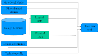
3. What are the inputs for floorplan?
A. The following are the inputs for Floorplan
4. What are the outputs of floorplan?
A. The following are the outputs for floorplan
5. What are the floorplaning
control parameters?
6.
What is the Aspect Ratio?
7.
What is core utilization?
8.
What is total chip
utilization?
9.
How macro placement is done
in floorplaning? or What are the guidelines for macro placement?
10.
What is blockage? What are
the different types of blockages? How these blockages are used in physical design?
11.
What is Halo? How it is
useful?
12.
What are the fly/flight
lines? How these fly/flight lines are useful during macroplacement ?
A.
Please visit
Macro Placement post
13.
A netlist consisting
of 500k gates and I have to estimate die area and floorplanning. How do I go about it?
A.
There are 2 methods to
estimate die area
Method 1:
Each cell has
got its area according to a specific library. Go through all your cells and
multiply each cell in its corresponding area from your vendor's library. Then
you can take some density factor - usually for a standard design you should
have around 80% density after placement. So from this data you can estimate
your required die area.
Method 2:
One more way of
doing it is, Load the design in the implementation tool, try to change the
floorplan ( x & y coordinates ) in a such a way that the Starting
utilization will be around 50% -to- 60%. Again, it depends on the netlist
quality & netlist completion status (like Netlist is 75%, 80% & 90%
completed).
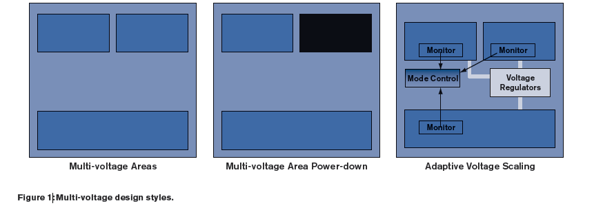
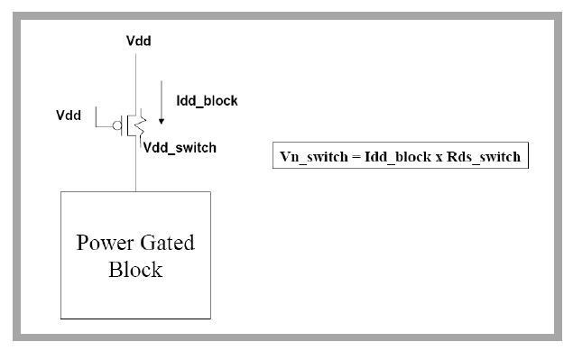
14.
How to do floor
planning for multi Vdd designs?
A.
First we have to decide
about the power domains, and add the power rings for each domain, and add the
stripes to supply the power for standard cells.
15.
How to calculate the
power ring width and power straps width and no of power straps using the core
power consumption?
16.
What is core
utilization percentage?
A. Core utilization percentage indicates the amount of core area
used for cell placement. The number is calculated as a ratio of the total cell
area (for hard macros and standard cells or soft macro cells) to the core area.
A core utilization of 0.8, for example, means that 80% of the core area is used
for cell placement and 20 percent is available for routing.
17. When core utilization area increased to 90%, macros got
placed outside core area so does it mean that increase in core utilization area
decreases width and height?
A. If you go on with 90% then there may be a problem of congestion
and routing problem. It means that you can’t do routing within this area.
Sometimes you can fit within 90% utilization but while go on for timing optimization like upsize and adding buffers will lead to increase in size. So
in this case you can’t do anything so we need to come back to floorplan again.
So to be on safer side we are fixing to 70 to 80% utilization.
18. Why do we remove all placed standard cells, and then write
out floorplan in DEF format. What's use of DEF file?
A. DEF deals only with floorplan size. So to get the abstract of
the floorplan, we are doing like this. Saving and loading this file we can get
this abstract again. We don’t need to redo floorplan.
19. Can area recovery be done by downsizing cells at path with
positive slack?
A. Yes, Area recovery can be done by downsizing cells at path with
positive slack. Also deleting unwanted buffers will also help in area recovery
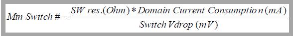
20. We can manipulate IR drop by changing number of power straps.
I increased power straps which reduced IR drop, but how many power straps can I
keep adding to reduce IR drop? How to calculate number of straps required. What
problems can arise with increase in number of straps?
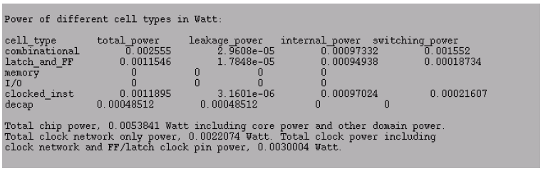
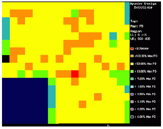
A. We can use tools to calculate IR drop (ex:- Voltagestrom,
Redhawk) if drop is high. Based on that we can add straps. But if you do projects
repeatedly you will come to know that this much straps is enough. In this case you
will not need tools. It’s having calculation but it’s not accurate it’s an
approximate one. Number of straps will create problem in routing also it
affects area. So results will be in routing congestion. To number of power
straps required for a design click here.
21. aprPGConnect, is used for logical connection of all VDD, VSS
nets of all modules. so how do we connect all VDD, VSS to global VDD /VSS nets before
placement?
A. The aprPGConnect, is used for logical connection of all VDD, VSS
nets of all modules. For physical
connection you can use the axgCreateStandardcellRails command to create the standard
cell rails and through them connect to the rings or the straps depending upon
power delivery design.
22. A design has memory and analog IP. How to arrange power and ground
lines in floor-plan. Is it separate digital and analog power lines? It is
important to design power-ground plan on ASIC?
A. Basically you have to make sure to keep analog and digital rails
isolated from one another. All hard macro and memory blocks need to have a vdd/vss
pair ring around them. Memories are always on the side or corners of your chip.
Put a pair of vdd/vss ring around your design. This is usually called core
power ring.
Create a pair of
vertical vdd/vss every 100 micron. This is called the power straps and on
either side taps into the core power ring. put a pair of vdd/vss around every
analog block and strap these analog rings (using a pair of vdd/vss) and run
them to your package vdd/vss rings.
Keep in mind
that in every place a digital vdd/vss crosses analog vdd/vss straps, then you
need to cut the digital vdd/vss on either side of the analog crossing to
isolate the analog from digital noise. you need to dedicate pins on your chip
for analog power and ground. Now we come to the most time consuming part of
this, HOW THICK SHOULD YOU MAKE all these rings/straps. The answer is this is
technology dependent. Look into the packaging documentations, they usually have
guidelines for how to calculate the thickness of you power rings. Some even
have applications that calculate all this for you and makes the cuts for
analog/digital crossings.
23. In my design, core PG ring and strips were implemented by
M6/M7,and strips in vertical orientation is M6.I use default method to connect
M6 strips to stand cell connection,M1,the vias from V12,V23,.. to V56 will
block the routing of M2,..M6, it will increase congestion to some extent. I
want to know is there any good method to avoid congestion when add strips or
connect strips to standard cell connection?
A. In Synopsys ICC, there was a command controlling the standard
cell utilization under power straps. Using this you can have some sort of
channels passing through stacked vias, between standard cells. This limits the
detours done because of these stacked vias and allows more uniform cell
placement resulting and a reduced congestion. in Soc Encounter, The command
setPrerouteAsObs can be used to control standard cell density under power
strips. But the 100% via connection from M1 to M6 under wide strip metal still
block other nets' routing.
124. How to control via
generation when do special route for standard cell, such as how to reserve gaps
between vias for other net routing?
A. To remove those stack vias you need to
1.
Either returns back to
floorplan step, where power straps and power/ground preroute vias are dropped.
Normally vias are dropped regularly to reduce power & ground resistance;
therefore maximum numbers of vias are dropped over power/ground nets. Therefore
you need to check your floorplan scripts. They should be after horizontal &
vertical power strap generation at M6 & M7.
2. If the vias to be removed
are at specific regions you can delete them at any step, but before global
routing of course to allow global route be aware of resources/obstructions. In
this case as you'll increase the power/ground resistance you should confirm
this methods validity by IR Drop analysis.
3. If IR Drop is an issue,
another option would be placing standard cell placement percentage blockages
(Magma has percentage blockages which is good at reducing blockages). This is
the safest method as you don't need to delete those stacked M1-to-M5 vias
anymore. However as you'll need to reduce placement density this will cost you
some unused area.
1 25. How to do a good floor plan and power stripes with blocks?
A. A good floorplan is made when:
-Minimum space
lost between macros/rows,
-Macros placed
in order to be close to their related logic,
-IR/Electro Migration
is good
-Routing
congestion as minimal.
126. How to reduce congestion?
A. By adding
placement blockage & routing blockage during the floorplan, Congestion can
be reduced. Placement blockage is to
avoid the unnecessary cell placement in between macros & other critical areas. Routing
blockage is used to tell the global router not to route anything on the particular area. Sometimes people used to
change/modify the blockages according to their needs at each
stage of the design.
Normally routing blockages should
be placed before global routing to force global router to respect these
blockages. Most Place and Route tools runs the first global routing at
placement step and then updates it incrementally, therefore add blockages before
placement. Otherwise if you want to use it after any global/detail routing is
done, you may need to update global routing first (may be incrementally).
27. How to find the reason for congestion in particular region? How
to reduce congestion?
A. First analyze placed congested database, and find out the hot
spot which is highly congested.
Case -1: "Congestion in Channel
between macro"
Reason:- Not enough tracks is available in channels
to route macro pins, or channel is highly congested because of std cell
placement.
Solution:- Need to increase
channel width between Macros or please make sure that soft blockage or hard
blockage is properly placed.
Case -2:- "Congestion
in Macro Corners"
Reason:- Corners of macro
is very prone to congestion because its having connectivity from both direction
Solution:-
1. Place some HALO around each
macro (5-7um).
2. Place a hard blockage on macro
corners (corner protection (Hard Placement Blockage) done after standard cell
rail creation otherwise it won't allow standard cell inside it.
Case -3: "Congestion
in center of chip/congestion in module anywhere in chip"
Reason:- Congestion in
standard cell or module is based on the module local density (local density is very high 95%-100%).Also depend on module nature (highly connected). Die area
less.
Solution:-
1. Module density should be even in whole chip (order os 65-85%).
2. Use density screen/Partial blockage to control module density in
specific areas.
3. Use cell padding
4. If congestion is too big in that case chip area should be increased
based on the congestion map.
28. What are the reasons for the Routing congestion in a design?
A. Routing congestion can be due to:
1. High standard
cell density in small area.
2. Placement of
standard cells near macros.
3. High pin
density on one edge of block.
4. Placing
macros in the middle of floorplan.
5. Bad Floorplan
6. Placement of
complex cells in a design
7. During IO
optimization tool does buffering, so lot of cells sits at core area.
29. What
actually happens in power planning? What is the main aim of power planning?
A.
The main aim of power planning is to ensure all the cells in the design are able
to get sufficient power for proper
functioning of the design. During the power planning the power rings and power
straps are created to distribute power equally across
the design.
Power straps are
provided for the regulated power supply throughout the block or chip. Number of straps depends on
the voltage and the current of your design. You must design the power grid that will provide
equal power from all sides of the block .you can also use the early rail
analysis method determine the IR
drop in your block and lay the sufficient power stripes.
30. How power stripes are useful in power planning ?
A. If the chip size is large, therefore core power rings
do not able to supply power to standard cells
because of long
distance particularly the cells in the center of the chips (or will give high
IR drop to
the farthest
cells), then you need power stripes. The number of stripes depend of
the area of you chip.
31. What is the minimum space
between two macros? How we can find minimum space of macros?
A. The distance between macro
= (no. of pins of macros*pitch*2)/no. of available routing layers
For example, the design has 2 macros having the
pins of 50 each macro and pitch = 0.50 and available
metals are 8.


