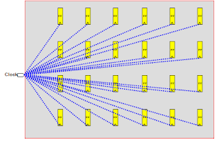
Clock Tree Synthesis (CTS) is the process of inserting buffers/inverters along the clock paths of the ASIC design to balance the clock delay to all clock inputs. So in order to balance the skew and minimize insertion delay CTS is performed. We will discuss about skew and insertion delay in upcoming posts. As shown in below figure 1, Before CTS, All clock pins are driven by a single clock source. Here we are discussing CTS overview. What are the checklist before CTS and after CTS?? What are the inputs and outputs for CTS? How CTS effect the design.
Checklist before CTS:
- Placement – Completed
- power ground nets – Prerouted
- Estimated Congestion – acceptable
- Estimated Timing – acceptable (~ 0 ns slack)
- Estimated Max Tran/Cap – No violations
- High Fanout Nets
Inputs required for CTS:
- Detailed Placement Database
- Target for latency and skew if specified
- Buffers or Inverters for building the clock tree
- Clock Tree DRC (Max Tran, Max Cap, Max fanout, Max no of buffer levels)
Output of CTS:
- Database with properly build clock tree in the design
Checklist after CTS:
- Skew Report
- Clock Tree Report
- Timing Reports for setup and hold
- Power and Area Report
CTS Goals:
- Minimizing Clock Skew
- Minimizing Insertion Delay
- Minimizing Power Dissipation
Why clock routes are given more priority than signal nets ? Clock is propagated after placement because the exact physical location of cells and modules are needed for the clock’s propagation which in turn impacts in dealing with accurate delay and operating frequency and clock is propagated before routing because when compared to signal routes, clock routes are given more priority. This is because; clock is the only signal switches frequently which in acts as source for dynamic power dissipation.
Effects of CTS:
- Clock Buffers are added
- Congestion may increase
- Non-clock cells may have been moved to less ideal locations
- Can introduce timing and max tran/cap violations


